July 2006
Rev 9
1/17
17
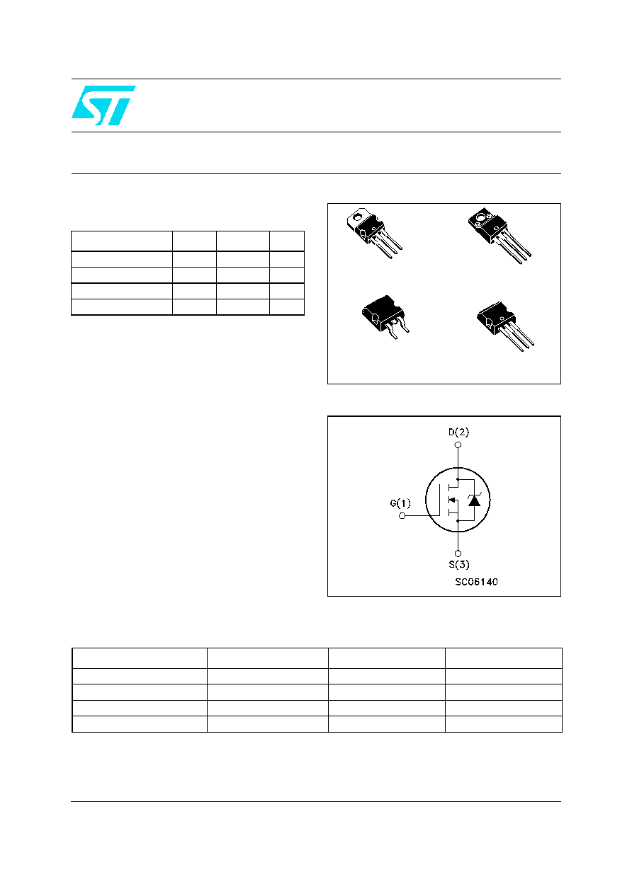
STB11NM60FD - STB11NM60FD-1
STP11NM60FD - STP11NM60FDFP
N-channel 600V - 0.40
- 11A - TO-220/TO-220FP/D
2
PAK/I
2
PAK
FDmeshTM Power MOSFET (with fast diode)
General features
100% avalanche tested
High dv/dt and avalanche capabilities
Low input capacitance and gate charge
Low gate input resistance
Tight process control and high manufacturing
yields
Description
The FDmeshTM associates all advantages of
reduced on-resistance and fast switching with an
intrinsic fast-recovery body diode. It is therefore
strongly recommended for bridge topologies, in
particular ZVS phase-shift converters.
Applications
Switching application
Internal schematic diagram
Type
V
DSS
R
DS(on)
I
D
STB11NM60FD
600V
<0.45
11A
STB11NM60FD-1
600V
<0.45
11A
STP11NM60FD
600V
<0.45
11A
STP11NM60FDFP
600V
<0.45
11A
TO-220
TO-220FP
D≤PAK
I≤PAK
D≤PAK
1
2
3
1
2
3
1
3
1
2
3
www.st.com
Order codes
Part number
Marking
Package
Packaging
STB11NM60FD
B11NM60FD
D≤PAK
Tape & reel
STB11NM60FD-1
B11NM60FD
I≤PAK
Tube
STP11NM60FD
P11NM60FD
TO-220
Tube
STP11NM60FDFP
P11NM60FDFP
TO-220FP
Tube

Contents
STB11NM60FD - STB11NM60FD-1 - STP11NM60FD - STP11NM60FDFP
2/17
Contents
1
Electrical ratings . . . . . . . . . . . . . . . . . . . . . . . . . . . . . . . . . . . . . . . . . . . . 3
2
Electrical characteristics . . . . . . . . . . . . . . . . . . . . . . . . . . . . . . . . . . . . . 4
2.1
Electrical characteristics (curves) . . . . . . . . . . . . . . . . . . . . . . . . . . . . 6
3
Test circuit . . . . . . . . . . . . . . . . . . . . . . . . . . . . . . . . . . . . . . . . . . . . . . . . 9
4
Package mechanical data . . . . . . . . . . . . . . . . . . . . . . . . . . . . . . . . . . . . 10
5
Packaging mechanical data . . . . . . . . . . . . . . . . . . . . . . . . . . . . . . . . . . 15
6
Revision history . . . . . . . . . . . . . . . . . . . . . . . . . . . . . . . . . . . . . . . . . . . 16
STB11NM60FD - STB11NM60FD-1 - STP11NM60FD - STP11NM60FDFP
Electrical ratings
3/17
1 Electrical
ratings
Table 1.
Absolute maximum ratings
Symbol
Parameter
Value
Unit
TO-220/
D≤PAK/I≤PAK
TO-220FP
V
DS
Drain-source voltage (v
gs
= 0)
600
V
V
DGR
Drain-gate voltage (R
GS
= 20 k
)
600
V
V
GS
Gate- source voltage
±30
V
I
D
Drain current (continuos) at T
C
= 25∞C
11
11
(1)
1.
Limited only by maximum temperature allowed
A
I
D
Drain current (continuos) at T
C
= 100∞C
7
7
(1)
A
I
DM
(2)
2.
Pulse width limited by safe operating area
Drain current (pulsed)
44
44
(1)
A
P
TOT
Total dissipation at T
C
= 25∞C
160
35
W
Derating factor
0.88
0.28
W/∞C
dv/dt
(3)
3.
I
SD
<11A, di/dt<400A/µs, V
DD
= 80% V
(BR)DSS
Peak diode recovery voltage slope
20
V/ns
V
ISO
Insulation winthstand voltage (dc)
--
2500
V
T
stg
Storage temperature
≠65 to 150
∞C
Table 2.
Thermal resistance
Symbol
Parameter
Value
Unit
TO-220
D≤PAK/I≤PAK
TO-220FP
R
thj-case
Thermal resistance junction-case Max
0.78
3.57
∞C/W
R
thj-a
Thermal resistance junction-ambient Max
62.5
∞C/W
T
l
Maximum lead temperature for soldering
purpose
300
∞C
Table 3.
Avalanche data
Symbol
Parameter
Value
Unit
I
AR
Avalanche current, repetitive or not-repetitive
(pulse width limited by T
j
max)
5.5
A
E
AS
Single pulse avalanche energy
(starting Tj = 25∞C, I
D
= I
AR
, V
DD
= 35V)
350
mJ
Electrical characteristics
STB11NM60FD - STB11NM60FD-1 - STP11NM60FD - STP11NM60FDFP
4/17
2 Electrical
characteristics
(T
CASE
=25∞C unless otherwise specified)
Table 4.
On/off states
Symbol
Parameter
Test conditions
Min.
Typ.
Max.
Unit
V
(BR)DSS
Drain-source breakdown
voltage
I
D
= 250 µA, V
GS
= 0
600
V
I
DSS
Zero gate voltage
Drain current (V
GS
= 0)
V
DS
= Max rating
1
µA
V
DS
=Max rating, T
C
=125∞C
100
µA
I
GSS
Gate-body leakage
current (V
DS
= 0)
V
GS
= ±30V
±100
nA
V
GS(th)
Gate threshold voltage
V
DS
= V
GS
, I
D
= 250µA
3
4
5
V
R
DS(on)
Static drain-source on
resistance
V
GS
= 10V, I
D
= 5.5A
0.40
0.45
W
Table 5.
Dynamic
Symbol
Parameter
Test conditions
Min.
Typ.
Max.
Unit
g
fs
(1)
1.
Pulsed: Pulse duration = 300 µs, duty cycle 1.5 %
Forward transconductance
V
DS
> I
D(on)
x R
DS(on)max,
I
D
= 5.5A
5.2
S
C
iss
Input capacitance
V
DS
= 25V, f = 1 MHz,
V
GS
= 0
900
pF
C
oss
Output capacitance
350
pF
C
rss
Reverse transfer
capacitance
35
pF
C
oss eq
(2)
2.
C
oss eq.
is defined as a constant equivalent capacitance giving the same charging time as C
oss
when V
DS
increases from 0 to 80% V
DSS
.
Equivalent output
capacitance
V
GS
= 0V, V
DS
= 0V to
400V
100
pF
R
G
Gate input resistance
f=1 MHz Gate DC Bias= 0
test signal level = 20mV
open drain
3
Q
g
Total gate charge
V
DD
= 400V, I
D
= 11A,
V
GS
= 10V
(see Figure 15)
28
40
nC
Q
gs
Gate-source charge
7.8
nC
Q
gd
Gate-drain charge
13
nC

STB11NM60FD - STB11NM60FD-1 - STP11NM60FD - STP11NM60FDFP
Electrical characteristics
5/17
Table 6.
Switching times
Symbol
Parameter
Test conditions
Min.
Typ.
Max.
Unit
t
d(on)
t
r
Turn-on delay time
Rise time
V
DD
= 250V, I
D
= 5.5A
R
G
= 4.7
V
GS
= 10V
(see Figure 14)
20
16
ns
ns
t
r(Voff)
t
f
t
c
Off-voltage rise time
Fall time
Cross-over time
V
DD
= 400V, I
D
= 11A,
R
G
= 4.7
, V
GS
= 10V
(see Figure 16)
10
15
24
ns
ns
ns
Table 7.
Source drain diode
Symbol
Parameter
Test conditions
Min
Typ.
Max
Unit
I
SD
Source-drain current
11
A
I
SDM
(1)
1.
Pulse width limited by safe operating area.
Source-drain current (pulsed)
44
A
V
SD
(2)
2.
Pulsed: Pulse duration = 300 µs, duty cycle 1.5 %
Forward on voltage
I
SD
= 11A, V
GS
= 0
1.5
V
t
rr
Q
rr
I
RRM
Reverse recovery time
Reverse recovery charge
Reverse recovery current
I
SD
= 11A, V
DD
= 50V
di/dt = 100A/µs,
(see Figure 19)
140
680
A
ns
nC
A
t
rr
Q
rr
I
RRM
Reverse recovery time
Reverse recovery charge
Reverse recovery current
I
SD
= 11A, V
DD
= 50V
di/dt = 100A/µs,
Tj=150∞C
(see Figure 19)
260
1600
13
ns
nC
A